PSOC5LP 5 Volts to 3.3 Volts Or Less
The PSOC5 can work with 5 volts or 3.3 volts, down to 1.7 volts. These voltages can exist simultaneously in the system. There are several ways to work with 5 volts and 3.3 volts in a system.
Different Voltage Domains
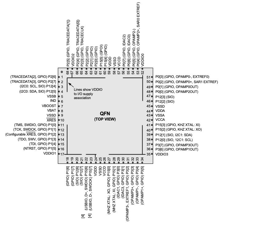
If you are designing the board layout from scratch, you can use the individual power supply domain pins on the PSOC. Below is a screenshot of a QFN 68 pin package from the datasheet for the part. The VDDIO0, VDDIO1, VDDIO2, VDDIO3 pins allow you to map the pins in that power domain to different voltages. Each one of these power domains can be a different voltage. Technically, the voltages can range from 1.2 volts to 5.5 volts.
The VDDA pin allows you to power the analog subsystem voltage from a completely different voltage. Note: the VDDA must be the highest voltage in the system. Note that if you are using VDDA of 5 volts, the analog pin’s corresponding VDDIO must also be 5 volts. Any over voltage input is clamped to the VDDIO supply using an internal diode, which is limited to 0.1 milliamps of current (100 microamps).
From the CY8C58LP Family datasheet, freely downloadable from Mouser, Digikey, etc. or Infineon (with registration) figure 2.3 shows the power domains for the QFN 68 pin package:
Non-Obvious Info
What is not obvious from this pin mapping is the fact the VDDIO pins are not the only voltage controls for I/O. SIO pins can be used for voltages higher than VDDA or VDDIO. These pins are marked as SIO on the graphic above. These SIO are pins P12[0] through P12[7]. They can run up to 5.5 volts in, regardless of VDDA/VDDIO in their domain.
If you look carefully at the graphic above, these SIO pins exist in each and every VDDIO section. This allows you to have each of the SIO pins sink 25 milliamps without damaging the part, within limits.
Warning: Total Current Limit For a VDDIO Section
While the SIO pins may be limited to 25 milliamps sink current (current to ground), the current sunk in a single VDDIO domain must be limited to 100 milliamps or less. The current sourced (from the VDD supply voltage) must also be less 100 milliamps or less. This limitation can bite you if you are not careful. Dead PSOCS are expensive PSOCS.
Special Voltage Inputs/Outputs Regardless of VDD FOR SIO
You may use one of the internal VDAC’s to set the threshold for a High/Low voltage on the SIO input. For Input voltage, this gives you a possibility of 8 more input comparators on the SIO pins, two at a time. This gives you a possibility of 12 analog comparators in the system.
For the output voltage control, you can use the VDAC to generate the “high” output voltage reference for the SIO pins. If you do this, you CANNOT use resistive pull up or down outputs on those pins. This is similar to the GPIO limit for USB pins.
Normal GPIO Tips/Tricks For 5V And 3V Mixes
If you don’t have an SIO available to you, and you are using one or more 3.3 volt parts with a 5 volt PSOC VDDIO, you have at least one more option. For output, you configure the Pins to be Open Drain Outputs, Pull Down, and (possibly) use a pull up resistor attached to the 3.3v supply so the resistor pulls the voltage to 3.3v for high, and the PSOC pin drives to ground for low. (Trick: In this case, if the Pin is set to a value of “1”, then it can be read by your program and its value (0 or 1) will follow the input voltage value. You can use the programmable threshold to set what the value of 1 is, but 50% of VDDIO (i.e. CMOS) is normal.)
If you use an external pull up resistor on that pin, you can then connect to a 3.3v device. The pull up resistor must be sized properly so as to not overload the port pin when driving the pin output to 0 volts. (4 or 8 milliamps to ground is usually the limit for a GPIO port, see the pin configuration inside PSOC Creator. So, a resistance of 2,000 to 3,000 ohms would be about right for 5 V VDDIO.) Using a resistor pull up along with total path capacitance generally limits the maximum I/O frequency. (Search Google for R/C Time Constant for more information.) You will have to experiment to see what that limit is.
USB I/O Pins For Different Purpose
You can use the USB I/O pins on the PSOC for GPIO, with limitations. First limitation is the USB I/O Pins are only powered from VDDD. That allows a VDDD of 5V (USB normal voltage max) use even when that section’s VDDIO is 3.3 volts, but that limits connecting to lower voltage devices in some cases. In most cases, you want to use 22 ohm resistors in series with your USB pins to provide the most protection for the part. In addition, if you decide to use the USB pins as GPIO, your choice of modes is limited to Open Drain and Strong Drive. You cannot use Resistive Pull Up/Down with those pins. I have a board where I can use these pins as either RS232 or USB, depending upon how the plug in connector is used in the final device. (Either/Or, not both, set by software at boot.)
Fini
The PSOC5 part is the most versatile MCU out there. The recent modern MCU’s are constrained by cost and lower voltage requirements. Lower cost equals less flexibility. For most MCU’s out there, a single pin is limited to 2 or 3 purposes. For the PSOC5, nearly any pin can be used for any purpose. The limitations apply to so few pins that I can almost always lay out a board based on easiest pin routing, get it back from the PCB fab, and then download my program, and remap functionality without regard to which I/O pin is being used.
Lower MCU voltages are problems for me. In my world, 100 volts with signals riding on top of it is normal, so interfacing to 5 volts is difficult enough. In addition, batteries come in a minimum of 1.5 volts up to several hundred volts. 3 volts or less becomes problematic, as noise signals are in that range. It is too bad the supply chain crunch, which promises to extend out several years, has put the PSOC5 on the back burner. (Read that to mean totally unavailable world wide.) Infineon is just hurting themselves. And us.
Enjoy!
About The Author
W Maxfield
Firmware/hardware Engineer for too many years.